
SUPERPACS technology
Advanced packaging for the next generation of space electronics
Future telecommunication, navigation and earth-observation satellites must process increasing volumes of data while operating within strict limits on mass, volume and power. Conventional electronic packages cannot provide the interconnection density needed to combine advanced processors, memories, radio-frequency functions and other specialised components efficiently.
Advanced System-in-Package (SiP) technology addresses this challenge by bringing multiple semiconductor dies together within a single compact module. Very short, high-density electrical connections can support faster data exchange with lower interconnection losses and lower energy consumption than links routed through a conventional package substrate. For space systems, however, these benefits must be combined with mechanical robustness, thermal management and reliable operation in harsh environments.
Enabling chiplet-based space systems
SUPERPACS enables chiplet architecture through advanced packaging. Instead of implementing every function in one large and highly complex semiconductor die, a system can be divided into smaller chiplets, each designed for a particular function or manufacturing technology. These chiplets are integrated side by side and interconnected through an intermediate routing structure called an interposer.
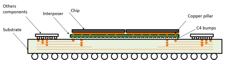
This modular approach can facilitate the combination of digital processing, high-bandwidth memory, radio-frequency conversion and other specialised functions in one package. The interposer provides the short, dense links required between chiplets, while the underlying package substrate supplies power and connects the complete System-in-Package to the spacecraft electronics. SUPERPACS will develop design rules starting from standardized chiplet-interconnect concepts and adapt them to advanced packaging requirements for space applications.
A two-fold technology approach
SUPERPACS develops and evaluates two complementary interposer technologies. This concurrent approach allows the project to investigate different balances between integration density, reliability, manufacturability and cost.
Silicon interposer
The silicon-interposer platform targets high-density and high-reliability integration. Fine multilayer routing connects chiplets over very short distances, while through-silicon vias provide vertical connections to the package substrate. The platform will also investigate the integration of passive electrical components, such as capacitors and resistors, within the interposer.
Silicon offers fine-feature processing, good dimensional stability and a coefficient of thermal expansion close to that of silicon chiplets. These properties make it attractive for demanding space applications. The principal challenges are controlling warpage and mechanical damage as the interposer becomes larger and thinner, managing the complexity of through-silicon-via fabrication and ensuring robust connections to the organic package substrate.
Ultra-high-density organic interposer
The organic-interposer platform seeks to combine fine-pitch chiplet integration with the flexibility and scalability of advanced IC-substrate manufacturing. It uses multilayer organic materials and semi-additive processing to create dense routing structures. Coreless and asymmetric constructions will be investigated to obtain thin interposers and place ultra-high-density routing only where it is needed.

Organic interposers offer a potentially adaptable and cost-effective route for complex packages, particularly when manufactured in panel formats. Their development nevertheless presents significant challenges. Organic materials are less dimensionally stable than silicon and may expand, shrink or deform during lamination and thermal processing. Achieving fine features across large panels therefore requires careful control of material behaviour, layer alignment, via formation and warpage.
From fine-pitch assembly to complete modules
Integrating chiplets involves more than manufacturing the interposer. Chiplets with closely spaced connections must be positioned and bonded with high accuracy. SUPERPACS will investigate thermo-compression bonding for die-to-interposer assembly, followed by controlled underfilling and inspection. The interposer can then be connected to the package substrate using an assembly process appropriate to its larger connection pitch.
Flatness is critical throughout this process. Excessive warpage can cause misalignment, open connections or short circuits. Temperature, pressure, bonding time, tooling, cleaning and the sequence of assembly operations must consequently be developed as one integrated manufacturing flow. Electrical simulation and inspection methods will be used to support process development and verify the assembled structures.
Designed for reliability in space
Space packaging must tolerate temperature variations, mechanical vibration and shock while maintaining electrical and structural integrity. Packages containing silicon, organic dielectrics, copper and solder experience internal stress because these materials expand differently with temperature. Potential consequences include interposer warpage, delamination and cracking of redistribution layers or solder joints. Organic materials must also be assessed for radiation-related degradation and outgassing in vacuum.
SUPERPACS combines physical testing with predictive multiphysics modelling. Thermal and thermo-mechanical models will identify critical stress concentrations and estimate the reliability of die-to-interposer, interposer-to-substrate and substrate-to-board connections. Material characterisation and experimental measurements will be used to improve and validate these models.
Because no single established standard currently covers the design and qualification of these complex space-grade System-in-Package technologies, SUPERPACS will define a tailored verification and qualification flow using relevant ESCC, ECSS and industry standards. Two design, manufacturing and test cycles will be used: the first to identify weaknesses and improve the technology, and the second to validate more complete demonstrators in a representative environment. Results will feed back into validated design rules and a Process Design Kit for future space applications.
Towards a European advanced-packaging capability
By developing silicon and organic interposers, fine-pitch assembly processes, reliability methods and reusable design rules within one coordinated workflow, SUPERPACS aims to establish a European pathway from materials and technology building blocks to validated System-in-Package modules. This will support more compact and capable space electronics while strengthening European competence and industrial resilience in advanced packaging.

